|
|
|
|
The use of a Scanning Tunneling Microscope not only enables the imaging of surfaces with atomic resolution but also allows the manipulation of surfaces on (almost) the same lateral scale.
Our research activities in this field are aiming for the development of a STM- based nanolithography at room temperature in materials of high technological relevance such as silicon or gold.
Because STM nanowriting is limited to atomically flat surfaces and the manipulation depth is only up to a few nanometers, we are using different kinds of Self-Assembled Monolayer (SAM) on organthiole or organosilane basis as ultrathin, organic resist layers which can be formed as highly ordered monomolecular films on preactivated surfaces like silicon or many rare metals.
The films are manipulated by STM writing in ultrahigh vacuum at enhanced tunneling parameters and the structure is subsequently transferred into the underlying substrate by selective wet etch procedures.
The resulting nanostructured surface is then analyzed by means of Atomic Force Microscopy (AFM) or Scanning Electron Microscopy (SEM).
An alternative approach of direct surface manipulation was investigated by applying UV laser-induced STM writing.
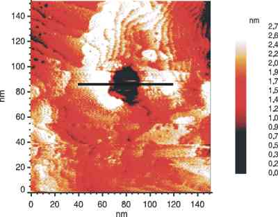
Smallest nanostructures could be achieved in Self-Assembled Monolayers adsorbed on single crystal surfaces. The first image shows an STM image of a Hexadecanethiol/Au(111) surface, in the center part a 20 nm * 20 nm scan area was manipulated at enhanced tunneling parameters. The edge accuracy of the structure is about 5 nm.
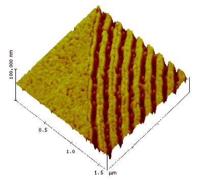
The next AFM image displays the part of a Au nanostructure as a result of STM lithography in Biphenylthiol and subsequent pattern transfer into gold by a cyanide etch. The typical line width of 55 nm (30 nm depth) is broadened by the isotropic etch characteristic of the wet etch process.
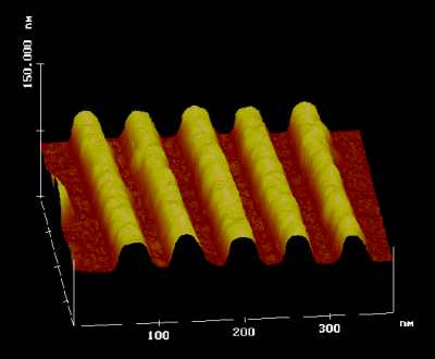
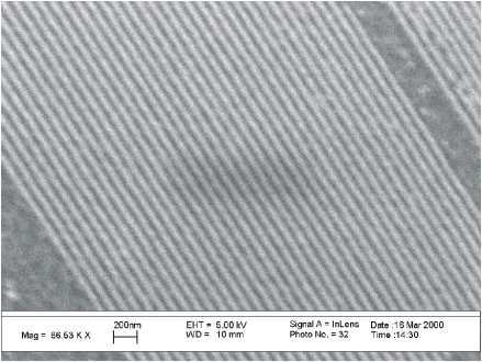
In Si(100), the anisotropic etch characteristic of a KOH was exploited for the fabrication of 35 nm wide and 30 nm deep grooves. The grating pattern was written in Octadecylthrichlorosilane (OTS) adsorbed onto hydroxilized Si(100). The AFM (left) and SEM (right) picture of the corresponding Si structure after etch transfer shows the high degree of periodicity achieved in the lithographic process. Future applications of these types of structures may be in the fields of microoptical elements (nanogratings) or complex nanofluidic devices.
See also:

|
Text von
Ulf Kleineberg
|
Letzte Änderung
23.11.2001 |
| Wir haben auf unseren Seiten Hyperlinks zu anderen Seiten im Internet gelegt, deren Webmaster wir nicht sind. Für alle diese Hyperlinks gilt: Wir erklären hiermit ausdrücklich, dass wir keinerlei Einfluss auf die Gestaltung und Inhalte dieser Seiten haben. Deshalb "distanzieren" wir uns hiermit von allen Inhalten dieser Seiten und machen uns ihre Inhalte in keiner Weise zu Eigen. | ||
|
©2001
Molekül- und Oberflächenphysik
Universität Bielefeld |
||